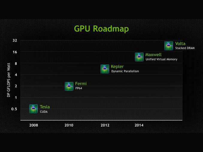
As we covered briefly in our live blog of this morning’s keynote, NVIDIA has publically updated their roadmap with the announcement of the GPU family that will follow 2014’s Maxwell family. That new family is Volta, named after Alessandro Volta, the physicist credited with the invention of the battery.
At this point we know very little about Volta other than a name and one of its marque features, but with how NVIDIA operates that’s consistent with how they’ve done things before. NVIDIA has for the last couple of years operated on an N+2 schedule for their public GPU roadmap, so with the launch of Kepler behind them we had been expecting a formal announcement of what was to follow Maxwell.
In any case, Volta’s marque feature will be stacked DRAM, which sees DRAM placed very close to the GPU by placing it on the same package, and connected to the GPU using through-silicon vias (TSVs). Having high bandwidth, on-package RAM is not new technology, but it is still relatively exotic. In the GPU world the most notable shipping product using it would be the PS Vita, which has 128MB of RAM in a wide-IO (but not TSV) manner. Meanwhile NVIDIA competitor Intel will be using a form of embedded DRAM for their highest-performance GT3e iGPU for their forthcoming Haswell generation CPUs.
The advantage of stacked DRAM for a GPU is that its locality brings with it both bandwidth and latency benefits. In terms of bandwidth the memory bus can be both faster and wider than an external memory bus, depending on how it’s configured. Specifically the close location of the DRAM to the GPU makes it practical to run a wide bus, while the short traces can allow for higher clockspeeds. Meanwhile the proximity of the two devices means that latency should be a bit lower – a lot of the latency is in the RAM fetching the required cells, but at the clockspeeds GDDR5 already operates at the memory buses on a GPU are relatively long, so there are some savings to be gained.
NVIDIA is targeting a 1TB/sec bandwidth rate for Volta, which to put things in perspective is over 3x what GeForce GTX Titan currently achieves with its 384bit, 6Gbps/pin memory bus (288GB/sec). This would imply that Volta is shooting for something along the lines of a 1024bit bus operating at 8Gbps/pin, or possibly an even larger 2048bit bus operating at 4Gbps/pin. Volta s still years off, but this at least gives us an idea of what NVIDIA needs to achieve to hit their 1TB/sec target.
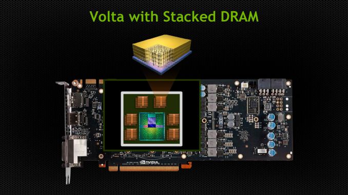
What will be interesting to see is how NVIDIA handles the capacity issues brought on by on-chip RAM. It’s no secret that DRAM is rather big, and especially so for GDDR. Moving all of that RAM on-chip seems unlikely, especially when consumer video cards are already pushing 6GB (Titan). For high-end GPUs this may mean NVIDIA is looking at a split RAM configuration, with the on-chip RAM acting as a cache or small pool of shared memory, while a much larger pool of slower memory is attached via an external bus.
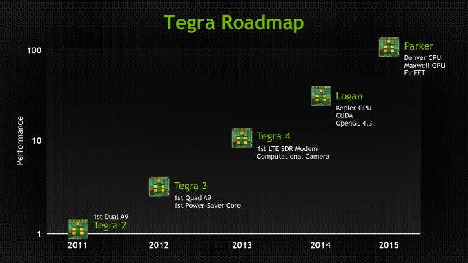
At this point Volta does not have a date attached to it, which is unlike Maxwell which originally had a 2013 date attached to it when first named. That date of course slipped to 2014, and while it’s never been made clear why, the fact that Kepler slipped from 2011 to 2012 is a reminder that NVIDIA is still tied to TSMC’s production schedule due to their preference to launch new architectures on new nodes. Volta in turn will have some desired node attached to its development, but we don’t know what at this time.
With TSMC shaking up its schedule in an attempt to catch up to Intel on both nodes and technology, the lack of a date ultimately is not surprising since it’s difficult at best to predict when the appropriate node will be ready 3 years out. On that note it’s interesting to note that while NVIDIA has specifically mentioned FinFET transistors will be used on their Parker SoC, they have not mentioned FinFET for Volta. Coming from their investor meeting the question came up, and while it wasn’t specifically denied we were also left with no reason to expect Volta to be using FinFET, so make of that what you will.
Meanwhile, in NVIDIA tradition they’ve also thrown out a very rough estimate of Volta’s performance by plotting their GPUs against a chart of FP64 performance per watt. Today Kepler is already at roughly 5.5 GFLOPS/watt for K20X, while Volta is plotted at 24ish. Like the rest of the GPU industry NVIDIA remains to be power constrained, so at equal TDPs we’d expect roughly four times the performance of K20X, which would put total FP64 performance at around 5 TFLOPS. But again, all of this is early into a GPU that will not be released for years.
Finally, while Volta is capturing the majority of the press due to the fact that it’s the newest GPU coming out of NVIDIA, this latest roadmap does also offer a bit more on Maxwell. Maxwell’s marque feature as it turns out is unified virtual memory. CUDA already has a unified virtual address space available, so this would seemingly go beyond that. In practice such a technology is important for devices integrating a GPU and a CPU onto the same package, which is what the AMD-led Heterogeneous System Architecture seeks to exploit. For NVIDIA their Parker SoC will be based on Maxwell for the GPU and Denver for the CPU, so this looks to be a feature specifically setup for Parker and Parker-like products, where NVIDIA can offer their own CPU integrated with a Maxwell GPU.